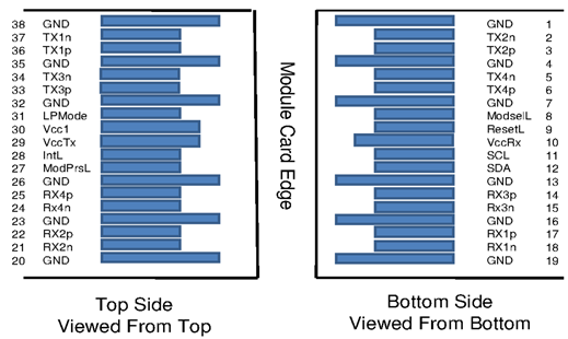
QSFP28 Pin Description
|
Pin |
Symbol |
Description |
Pin |
Symbol |
Description |
|---|---|---|---|---|---|
|
1 |
GND |
Ground |
20 |
GND |
Ground |
|
2 |
Tx2n |
Transmitter Inverted Data Input |
21 |
Rx2n |
Receiver Inverted Data Output |
|
3 |
Tx2p |
Transmitter Non-Inverted Data Input |
22 |
Rx2p |
Receiver Non-Inverted Data Output |
|
4 |
GND |
Ground |
23 |
GND |
Grounds |
|
5 |
Tx4n |
Transmitter Inverted Data Input |
24 |
Rx4n |
Receiver Inverted Data Output |
|
6 |
Tx4p |
Transmitter Non-Inverted Data Input |
25 |
Rx4p |
Receiver Non-Inverted Data Output |
|
7 |
GND |
Ground |
26 |
GND |
Ground |
|
8 |
ModSelL |
Module Select |
27 |
ModPrsL |
Module Present |
|
9 |
ResetL |
Module Reset |
28 |
IntL |
Interrupt |
|
10 |
Vcc Rx |
+3.3V Power Supply Receiver |
29 |
Vcc Tx |
+3.3V Power Supply Transmitter |
|
11 |
SCL |
2-wire Serial Interface Clock |
30 |
Vcc1 |
+3.3V Power Supply |
|
12 |
SDA |
2-wire Serial Interface Data |
31 |
LPMode |
Low Power Mode |
|
13 |
GND |
GND |
32 |
GND |
Ground |
|
14 |
Rx3p |
Receiver Non-Inverted Data Output |
33 |
Tx3p |
Transmitter Non-Inverted Data Input |
|
15 |
Rx3n |
Receiver Inverted Data Output |
34 |
Tx3n |
Transmitter Inverted Data Input |
|
16 |
GND |
Ground |
35 |
GND |
Ground |
|
17 |
Rx1p |
Receiver Non-Inverted Data Output |
36 |
Tx1p |
Transmitter Non-Inverted Data Input |
|
18 |
Rx1n |
Receiver Inverted Data Output |
37 |
Tx1n |
Transmitter Inverted Data Input |
|
19 |
GND |
Ground |
38 |
GND |
Ground |
QSFP28 Module Pad Layout
SFP28 Pin Description
|
Pin |
Connector Pin Name |
Port A Signal Name |
|
1 |
VeeT |
Module Transmitter Ground |
|
2 |
Tx_Fault |
Module Transmitter Fault |
|
3 |
Tx_Disable |
Transmitter Disable. Turns off transmitter laser output |
|
4 |
SDA |
2-wire Serial Interface Data Line |
|
5 |
SCL |
2-wire Serial Interface Clock |
|
6 |
Mod_ABS |
Module Absent. Grounded within the module |
|
7 |
RS0 |
Rate Select 0, optionally controls SFP+ module receiver |
|
8 |
Rx_LOS |
Receiver Loss of Signal Indication |
|
9 |
RS1 |
Rate Select 1, optionally controls SFP+ module transmitter |
|
10 |
VeeR |
Module Receiver Ground |
|
11 |
VeeR |
Module Receiver Ground |
|
12 |
RD- |
Receiver Inverted Data Output |
|
13 |
RD+ |
Receiver Non-Inverted Data Output |
|
14 |
VeeR |
Module Receiver Ground |
|
15 |
VccR |
Module Receiver Power Supply |
|
16 |
VccT |
Module Transmitter Power Supply |
|
17 |
VeeT |
Module Transmitter Ground |
|
18 |
TD+ |
Transmitter Non-Inverted Data Input. AC coupled |
|
19 |
TD- |
Transmitter Inverted Data Input. AC coupled |
|
20 |
VeeT |
Module Transmitter Ground |
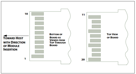
SFP28 Module Pad Layout
SFP to QSFP Pin Description
The below details the status/control signals interconnection between QSFP and the SFP connectors.
SFP to QSFP Status/Control Signals
|
QSFP Signal |
SFP Signal |
Description of Function |
|---|---|---|
|
ModPrsL |
ModAbs |
Connected to Vee inside the SFP transceiver. |
|
IntL |
Rx_LOS |
Inverted logic: IntL = Rx_LOS OR Tx_FAULT |
|
Tx_Fault |
||
|
ModSelL |
|
Used for encoding of the mutual exclusive SCL/SDA switch enable logic as shown below. |
|
LPMode |
RS0 |
Inverted logic: RS0 = RS1 = NOT LPMode |
|
RS1 |
||
|
ResetL |
Tx_Disable |
Inverted logic: Tx_Disable = NOT ResetL |
|
SCL |
SCL |
Connected to mutual exclusive bidirectional switches using the encoding shown in below. |
|
SDA |
SDA |
Connected to mutual exclusive bidirectional switches using the encoding shown in below. |
SFP to QSFP (Patented U.S. Pat. 7,934,959)
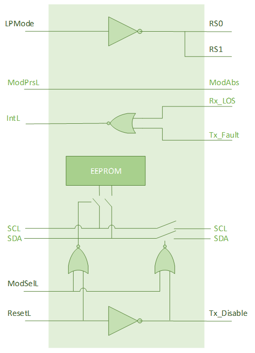
The mutually exclusive SDA/SCL connections to the QSA EEPROM and SFP module are controlled by the ModSelL and ResetL signals:
|
ModSelL |
ResetL |
QSA EEPROM Access |
SFP Access |
|---|---|---|---|
|
0 |
0 |
Yes |
No |
|
0 |
1 |
No |
Yes |
|
1 |
0 |
No |
No |
|
1 |
1 |
No |
No |
Last updated: